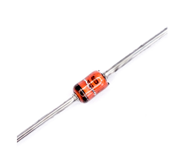
Zener diodes are heavily doped semiconductor diodes designed to operate in the reverse direction. Diodes that are specifically designed to optimize the breakdown area are called Zener diodes. Also called a breakdown diode.
Zener diodes behave like regular forward-biased p-n junction diodes. When a Zener diode is forward-biased, it allows large currents and blocks only small currents.
Zener diodes are more heavily doped than regular PN junction diodes. So we have a very thin depletion region. Therefore, Zener diodes can carry more current than regular p-n junction diodes. The voltage drop across the diode also remains constant over a wide voltage range. This is the feature that makes Zener diodes suitable for use in voltage regulation.

V-I Characteristics of Zener Diode
The figure below shows the VI characteristics of a Zener diode. When a Zener diode is forward-biased, it behaves like a normal diode. However, when a reverse-biased voltage is applied to the Zener diode, it behaves differently. When a reverse bias voltage is applied to the Zener diode, only a small amount of leakage current is allowed until the voltage drops below the Zener voltage. When the reverse voltage across the Zener diode reaches the Zener voltage, a large current begins to flow. At this point, a slight increase in reverse voltage causes a rapid increase in current. This sudden increase in current causes a breakdown called Zener breakdown. However, Zener diodes exhibit controlled breakdown and damage the device.

Symbol of Zener Diode

Working of Zener Diode
Zener diodes add high levels of impurities to the semiconductor material to make it more conductive. The presence of these impurities makes the depletion region of the diode very thin. The electric field strength increases in the depletion region due to heavy doping even when a small voltage is applied.
When the Zener diode is unbiased, electrons accumulate in the valence band of the p-type semiconductor material and no current flows through the diode. The band in which valence electrons are located is called valence band electrons. Electrons readily move from one band to another when external energy is applied across the valence band.
When the diode is reverse-biased, the electric field strength increases across the depletion region. Therefore, electrons are free to move from the valence band of the P-type semiconductor material to the conduction band of the N-type semiconductor material. Once the depletion region is completely removed, the diode will start conducting current in the reverse bias direction.
Specification of Zener Diode
The specifications for commonly used Zener diodes are:
- Zener/Breakdown Voltage – The Zener or reverse breakdown voltage ranges from 2.4V to 200V, with a maximum of 47V for surface mount devices, but can reach 1kV.
- Current Iz (max) – This is the maximum current at the rated Zener voltage (Vz – 200 μA to 200 A).
- Current Iz (min) – This is the minimum current required for the diode to break down.
- Power Rating – Indicates the maximum power that the Zener diode can dissipate. It is the product of the diode voltage and the current through the diode.
- Temperature Stability – Diodes around 5V are the most stable.
- Voltage Tolerance – It is typically ±5%.
- Zener Resistance (Rz) – The resistance exhibited by the Zener diode.
Types of Zener Diode
Zener diodes can be classified based on several parameters:
- Nominal Voltage
- Maximum Reverse Current
- Power Dissipation
- Packaging Type
- Forward Drive Current
- Forward Voltage
Advantages of Zener Diode
- Very high power loss
- High precision
- Overflow current control
- Circuit voltage can be changed and stabilized
- Provides high performance
- Protects against overvoltage
Disadvantage of Zener Diode
- This diode is not suitable for large load currents
- The DC output voltage can change slightly with the Zener resistor.
- The output voltage is not adjustable
- As the load current changes, the Zener current changes.
- Less voltage regulation
- The high internal impedance of the circuit
Applications of Zener Diode
- Voltage Regulation
- Voltage Reference
- Over-voltage protection
- Switch between applications
- Clipper Circuit
