
Tunnel diodes, also known as Esaki diodes, are a type of diode consisting of a heavily doped semiconductor PN junction that reduces current as voltage increases due to negative resistance. This phenomenon is also called electron tunneling.
Japanese physicist Leo Esaki invented a new type of diode in 1957 by increasing the doping concentration of his PN junction diode. In doing so, he observed a “negative resistance” due to a “quantum-mechanical effect” he called “electron tunneling.” He won the Nobel Prize for his discovery of the electron tunneling effect. That is why the diode was called tunnel diode or Esaki diode. It has a negative resistance which means that current decreases as voltage increases within the operating range. It has used in high frequency applications due to their fast switching capability.
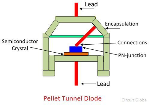
Construction of Tunnel Diode
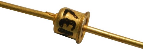
The device consists of two terminals, an anode and a cathode. The p-type semiconductor functions as the anode and the n-type semiconductor material functions as the cathode. Gallium arsenide, germanium and gallium antimonide are used in the manufacture of tunnel diodes.
The ratio of peak forward current value to valley current value is largest for germanium and smaller for silicon. Therefore, no silicon is used to manufacture the tunnel diodes. The doping density of tunnel diodes is 1000 times higher than that of ordinary diodes.
Symbol of Tunnel Diode

VI Characteristics of Tunnel Diode
In forward biasing, the heavy doping causes instantaneous conduction in the diode. The current in the diode reaches its maximum value Ip when a voltage Vp is applied across the diode. As the voltage continues to rise, the current through the terminals will decrease. And decreases until it reaches a minimum value. This minimum current value is called the valley current Iv.

The graph above shows that the current value decreases as the voltage increases from point A to point B. Therefore, graphs A to B show the range of negative resistance for tunnel diodes. This area shows the most important characteristics of the diode. In this region, the tunnel diode generates power instead of absorbing it.
Working of Tunnel Diode
Step 1: Unbiased tunnel diode
In unbiased tunnel diode, no voltage across the tunnel diode has applied. Due to the heavy doping, the conduction band of n-type semiconductors overlaps the valence band of p-type materials. The electrons from the n side and the holes from the p side overlap and have the same energy level.
Some electrons tunnel from the n-type conduction band to the p-type valence band with increasing temperature. Similarly, holes move from the valence band of the p region to the conduction band of the n region. Equal numbers of electrons and holes flow in opposite directions, resulting in a net current of zero.

Step 2: Small Voltage Applied to the Tunnel Diode
If a small voltage is applied across the tunnel diode that is less than the built-in voltage of the depletion layer, no forward current will flow through the junction.
However, a few electrons in the n-type conduction band tunnel to empty states in the p-type valence band. This creates a small forward bias tunneling current. Thus, a tunnel current begins to flow with the application of a small voltage.

Step 3: Applied voltage is slightly increased
When the voltage applied to the tunnel diode is slightly increased will create a large number of free electrons on the n-side and holes on the p-side. As the voltage increases, the overlap between the conduction and valence bands increases.
In simply, the energy level of the n-side conduction band is exactly equal to the energy level of the p-side valence band. As a result, maximum tunnel current flows.

Step 4: Applied voltage is further increased
A further increase in the applied voltage causes a small deviation of the conduction and valence bands.
Because the conduction band of n-type material and the valence band of p-type material still overlap. Electrons tunnel from the n-type conduction band to the p-type valence band and a small current flows. Therefore, the tunnel current begins to decrease.

Step 5: Largely Increased Voltage Applied to the Tunnel Diode
The tunneling current becomes zero when the applied voltage increases significantly. At this point, the conduction and valence bands no longer overlap and the tunnel diode behaves like a normal pn junction diode.

When this applied voltage is greater than the built-in potential of the depletion layer, normal forward current begins to flow through the tunnel diode.
The section of the curve where the current decreases with increasing voltage is the negative resistance region of the tunnel diode. Negative resistance range is the most important and most common characteristic of tunnel diodes.
Applications
- Oscillator
- Logic memory storage devices
- FM receivers
- Ultra high-speed switch
- Microwave circuit
- Amplifiers
- Solid-state circuits.